
3 Input Nand Gate Circuit Diagram
Here is some basic VHDL logic: 1. 2. signal and_gate : std_logic; and_gate <= input_1 and input_2; The first line of code defines a signal of type std_logic and it is called and_gate. Std_logic is the type that is most commonly used to define signals, but there are others that you will learn about.
Circuit Diagram Of Xnor Gate Using Nand Gates Only Wiring Diagram
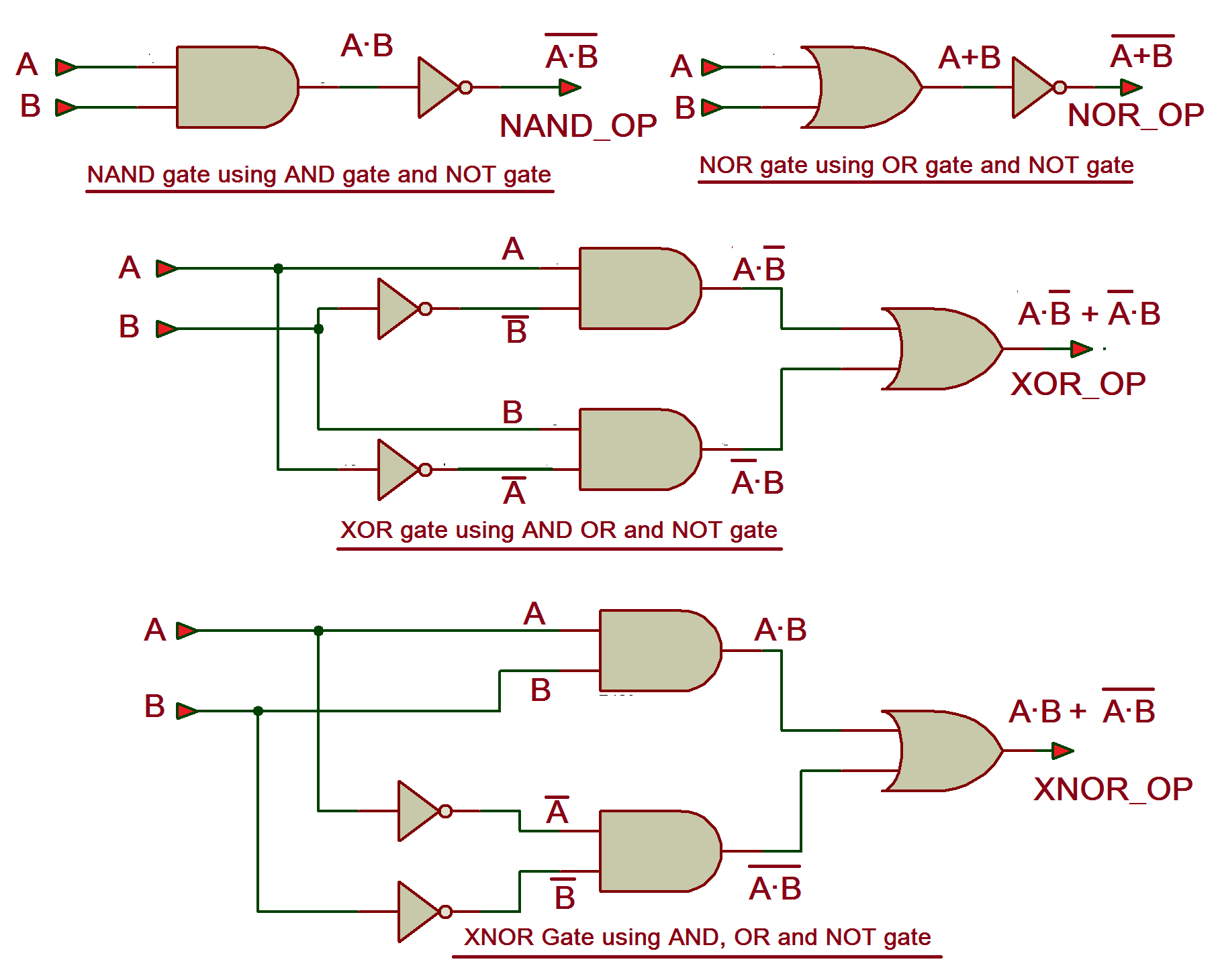
Logic gates are the building blocks of digital electronics.Digital electronics employ boolean logic. And logic gates are the physical circuits that allow boolean logic to manifest in the real world.. In this post, we will take a look at implementing the VHDL code for all logic gates using dataflow architecture.First, we will take a look at the logic equations of all the gates and then the syntax.

Implementation of Basic Logic Gates using VHDL in ModelSim
By Ashutosh Bhatt In the previous VHDL tutorial 4, we designed and simulated all seven logic gates (AND, OR, NOT, NAND, NOR, XOR, and XNOR) in VHDL. (If you are not following this VHDL tutorial series one by one, please go through all previous tutorials of these series before going ahead in this tutorial) In this tutorial,

Threeinput NAND gate, its graph representation and its leakage current
In FPGAs, there are no gates at all, just 4/5/6 input Look up tables (depending on the chip). With more inputs, you can produce more "gates" per lut. Reactions: verylsi
VHDL Tutorial 4 design, simulate and verify all digital GATE (AND
The code is compiled, and the input values are forced to simulate the NOT gate as shown below. Now that all the input combinations for A (0,1) are forced to the input signals, move the cursor throughout the waveform graph from 0ps to 500ps.. VHDL Code for NAND Gate: The output of the NAND Gate is nothing but the compelemnt of the AND Gate.
VHDL Tutorial 7 NAND gate as universal gate using VHDL
Write the VHDL code to implement a NAND gate with 3 inputs. Submitted by Monique F. Feb. 08, 2023 03:07 p.m. Instant Answer Step 1/2 First, we need to declare the inputs and outputs of the NAND gate.
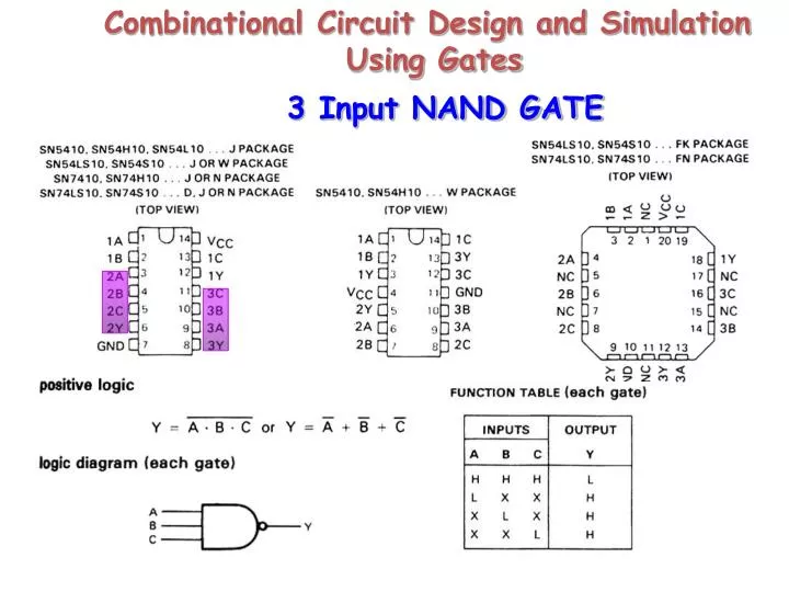
PPT 3 Input NAND GATE PowerPoint Presentation, free download ID4439271
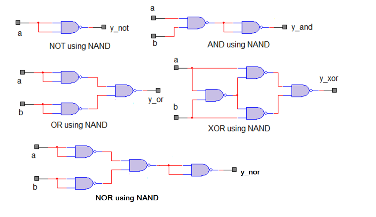
For the full code, scroll down. As evident, the logic circuit of an EXOR using NAND employs 4 NAND gates, two inputs, and a solitary output. Remember these details. Additionally, take a look at all the inputs to each of the gates. If you recall from our previous post on the VHDL code for a full adder using structural modeling.

SOLUTION Nand gate 2 input 3 input vhdl code Studypool
VHDL Logic gates coding. The basic "nand" gate: truth table equation symbol a b | c ----+-- c = a nand b; VHDL c = not ( a and b. 0 0 0 0 0 0 0 0 1 1 1 1 1 1 1 1 Notice that for two input variables, a b, there are 2^2 = 4 rows Notice that for four rows there are 2^4 = 16 columns. A question is: Which are "universal" functions from which.

Introduction to NAND Gate projectiot123 Technology Information
Example VHDL Code • 3 sections to a piece of VHDL code • File extension for a VHDL file is .vhd • Name of the file should be the same as the entity name (nand_gate.vhd) [OpenCores Coding Guidelines] LIBRARY DECLARATION ENTITY DECLARATION ARCHITECTURE BODY LIBRARY ieee; USE ieee.std_logic_1164.all; ENTITY nand_gate IS PORT(

2 Complementary CMOS threeinput NAND gate. Download Scientific Diagram
Created on: 12 December 2012 In the previous tutorial, we looked at AND gates, OR gates and signals in VHDL. This tutorial covers the remaining gates, namely NAND, NOR, XOR and XNOR gates in VHDL. NAND and NOR Logic Gates in VHDL NAND Gate The VHDL nand keyword is used to create a NAND gate: NAND Gate with Truth Table and VHDL NOR Gate

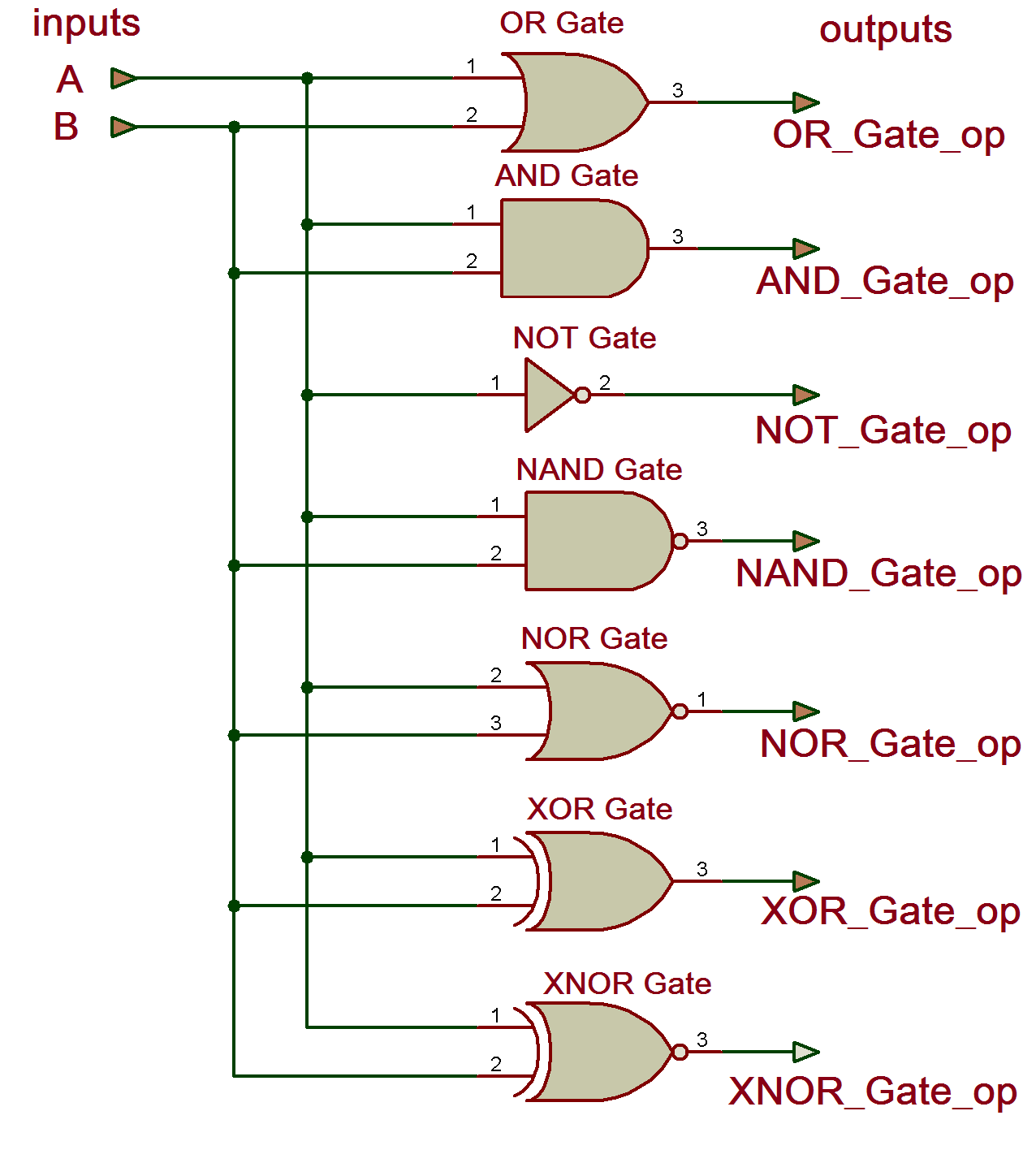
Experiment writevhdlcodeforrealizealllogicgates Coding, Logic
This tutorial on Multiple Input Gates in Verilog and VHDL accompanies the book Digital Design Using Digilent FPGA Boards - VHDL / Active-HDL Edition which co.
3inputNANDgate Multisim Live
$10 Udemy Course Coupon of above Course (from Basic to Advance Design with VHDL in VIVADO): https://www.udemy.com/vhdl-programming-with-xilinx-vivado-and-zyn.

Instances of VHDL gate family a) 2input AND gate, and b) 3input OR
Synthesizable VHDL code for two-input XOR logic. Full size image. Table 2.7 Truth table for two-input XOR logic. Full size table. Note XOR gate can be implemented by using two-input NAND gates. The number of two-input NAND gates required to implement two-input XOR gate are equal to 4. XOR gates are used to implement arithmetic operations like.
Logic NAND Gate
Ashutosh Sharma | Published January 29, 2020 | Updated April 17, 2020 Let's look into designing the NAND logic gate using all the three modeling styles in Verilog, i.e. Gate Level, Dataflow, and Behavioral modeling. The three different methods of modeling are based on the levels of abstraction.

VHDL code for NAND gate using Data Flow modeling YouTube
The architecture of VHDL code is written in three different coding styles : Dataflow Modelling Behavioral Modelling Structural Modelling 1. Logic Development for AND Gate: The AND logic gate can be realized as follows - The truth table for AND Gate is:

CircuitVerse 3 input NAND to 2 input NAND
In VHDL, a 74HC10 IC contains three 3-input NAND gates. (a) Write an entity declaration for the design entity triple_3 that is functionally equivalent to a 74HC10. (b) Write an architecture in the dataflow style for the design entity triple_3. Use only signal assignment statements with Boolean equations.